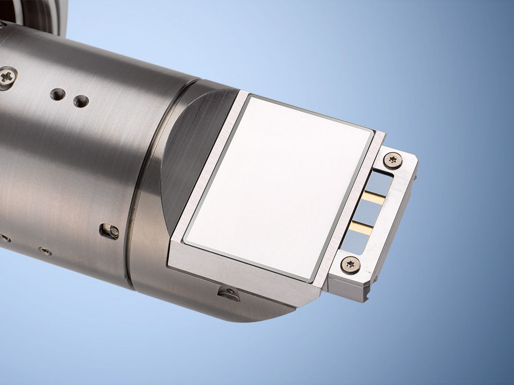
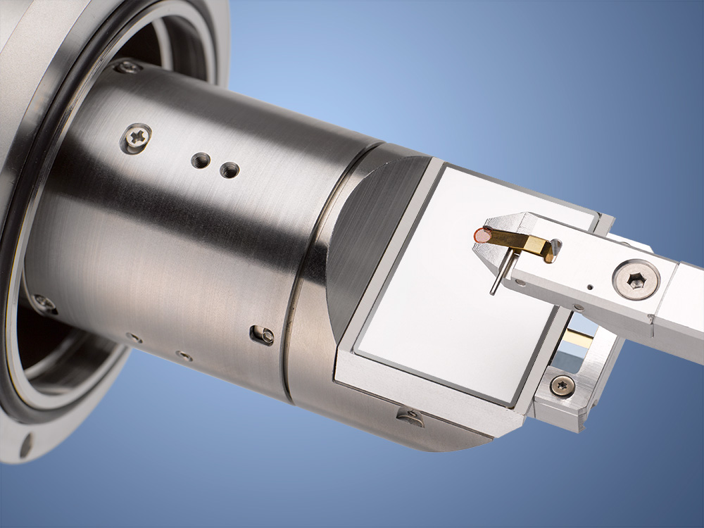
OPTIMUS TKD detector head
The high performance eFlash brookeEBSDSeries detector now configurable OPTIMUS ™ TKD probe.OPTIMUS™TKD 探头专为 SEM 中同轴透射菊池衍射分析(同轴 TKD)最佳的样品与探测器几何构型而设计。OPTIMUS ™ TKD 探头具有无与伦比的灵敏度,不仅可以采集菊池花样,甚至还可以提供类似 SAED(选区The design of electron diffraction).
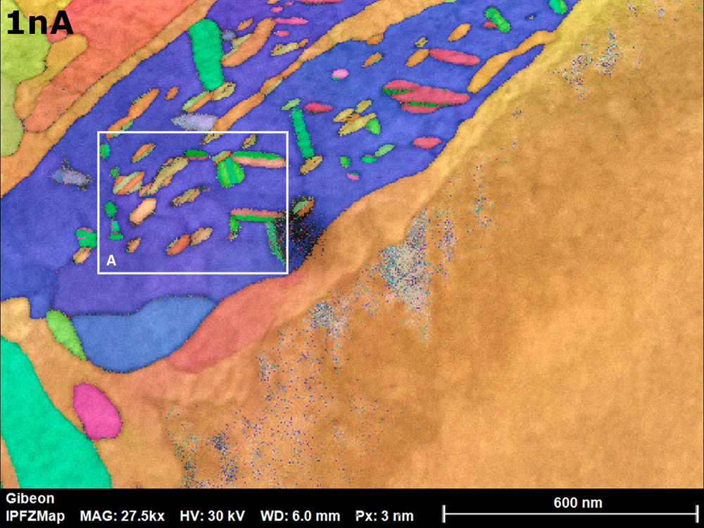
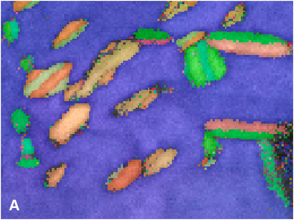
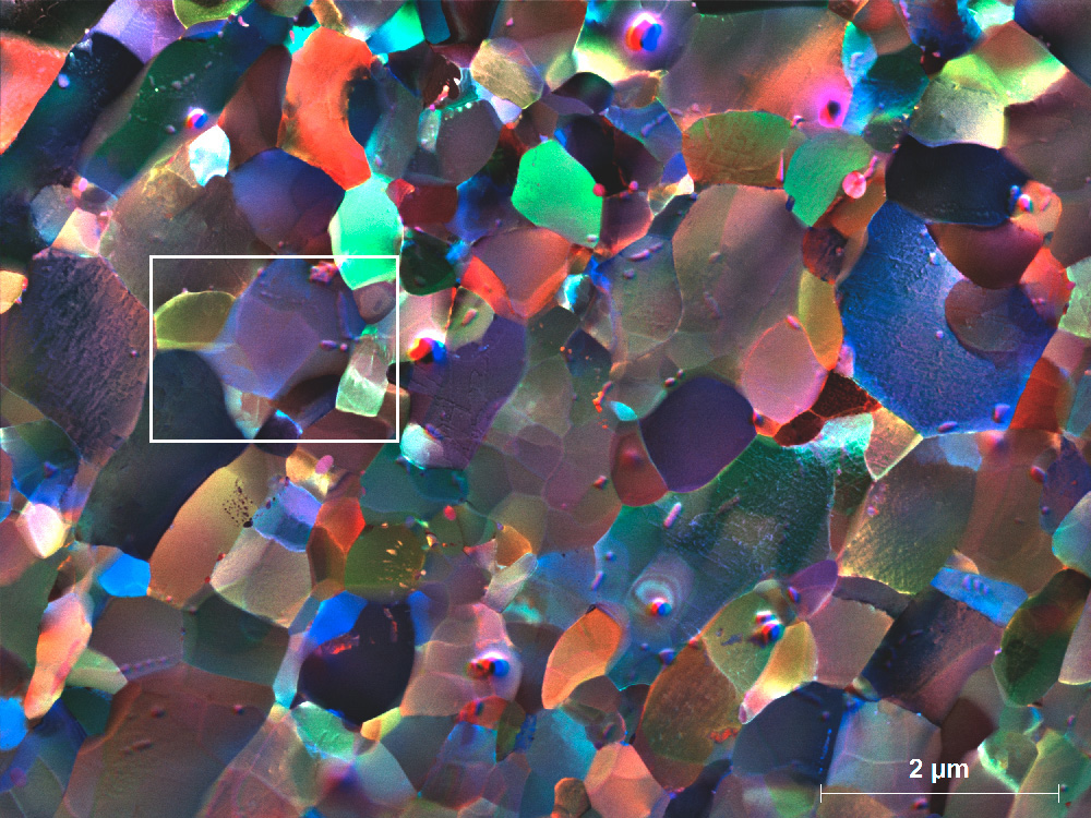
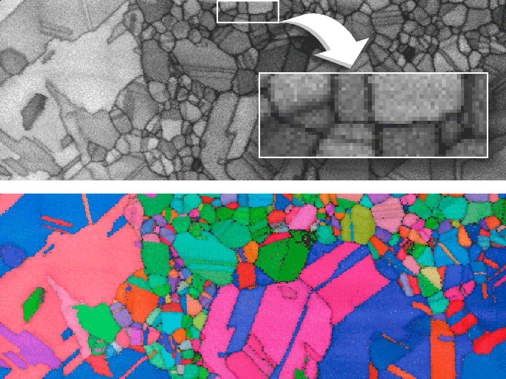
At least 2 nm distribution of grain oriented spatial resolution
Compared with vertical phosphor screen Settings, in the sample below the level of the phosphor screen has two main advantages:
- Signal strength increased by one order of magnitude
- Kikuchi patterns were less distortion
Stronger signal, can let us choose to gather light column orientation distribution, so as to improve the spatial resolution.Coaxial TKD experimental data of various materials, the results show that when using high-end FE - SEM, its effective spatial resolution can be up to 2 nm even better.At the same time, under the low acceleration voltage (kV) 5 coaxial TKD test is possible.Low voltage is helpful to reduce the mean free path, by raising the kikuchi diffraction semaphore.In the analysis of thin samples and "light" is very useful when the sample.In addition, Mr. Kikuchi patterns caused by gnomonic projection distortion is a common problem in the EBSD, especially influence use vertical phosphor screen to collect signals of off-axis TKD technology.
However, for OPTIMUS ™ TKD, phosphorus exactly match the center of the screen and design center, the optimal geometric configurations, even in terms of signal acquisition is better than conventional EBSD geometric configurations.Finally collected kikuchi patterns virtually no distortion, which significantly improves the detection of kikuchi bands and then the calibration accuracy.
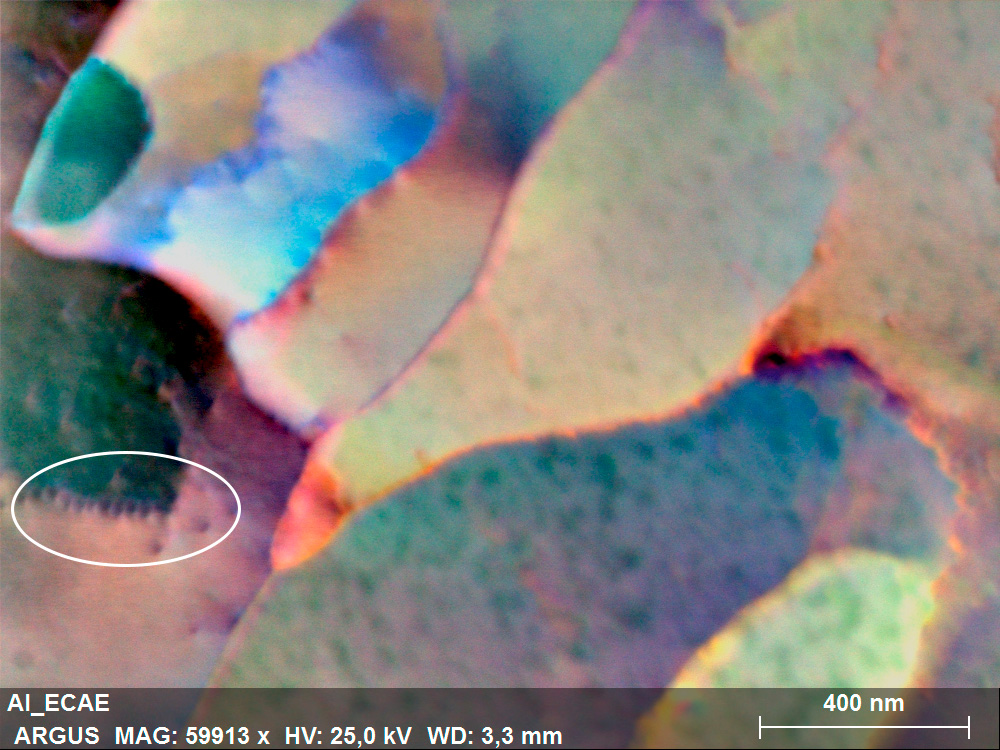
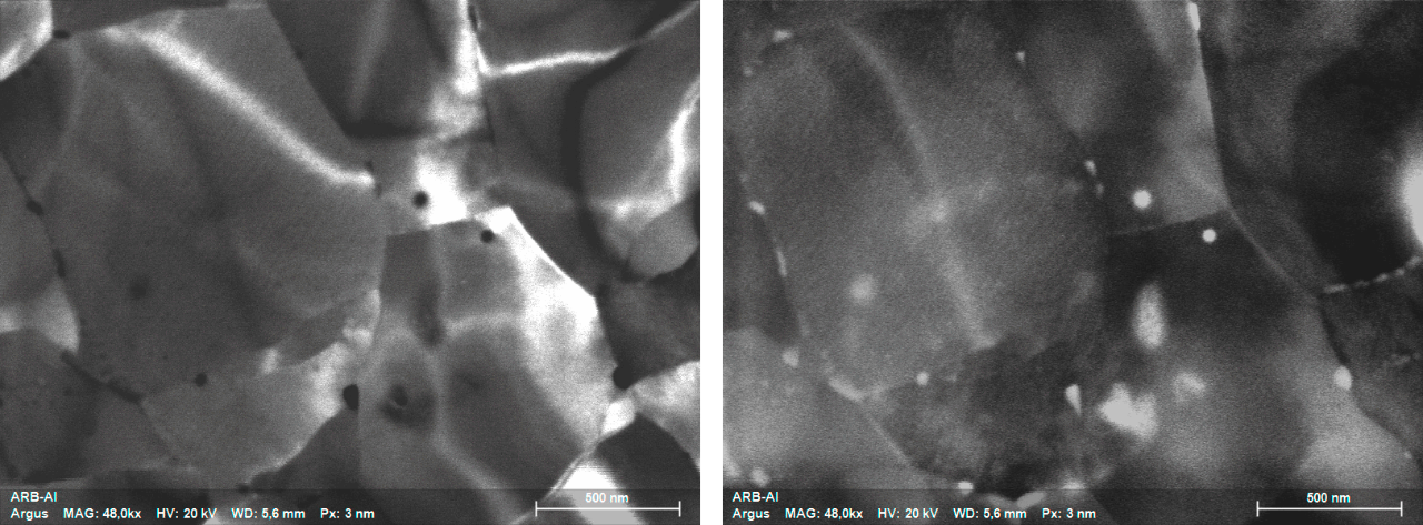
AGUS ™FSE imaging system
OPTIMUS™TKD equipped withARGUS ™™Imaging system, which can realize jing Ming field like kind of dark field image and class, image details can be up to the nanometer scale, almost turn your SEM in practice for "low voltage version of the TEM.ARGUS™But in deformation of material can be used to display a single dislocation and dislocation network.Kind of dark field like images can show more grain boundary surface position and Angle of 3 d information.
Ease of use
Each of the existingeFlashThe probe can be equipped with OPTIMUS™™ TKD detector head.Well-trained users can easily finish in 10 to 15 minutes.This allows the EBSD and TKD anytime and anywhere easily quickly switch between modes.OPTIMUS™TKD the collision protection system with advanced brooke: during the collision of unlikely, the detectors will back at the speed of 10 mm/s immediately, so as to significantly reduce the risk of any damage.OPTIMUS™TKD detector head and brooke SEM TKD professional toolkit seamless integration, including sampling frame, XFlash TKD®EDS detector series, used in synchronous measurement and ESPRIT 2 TKD/EDS analysis software.