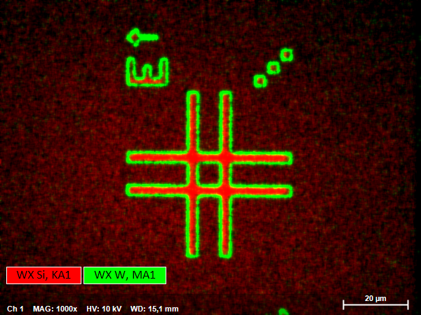
Semiconductor microchips material elements of the recognition
Conductive ceramic material tungsten silicide is often used in microelectronics, such as microchips.Tungsten silicide may as refractory in the semiconductor material, such as tungsten silicide on the silicon wafer.
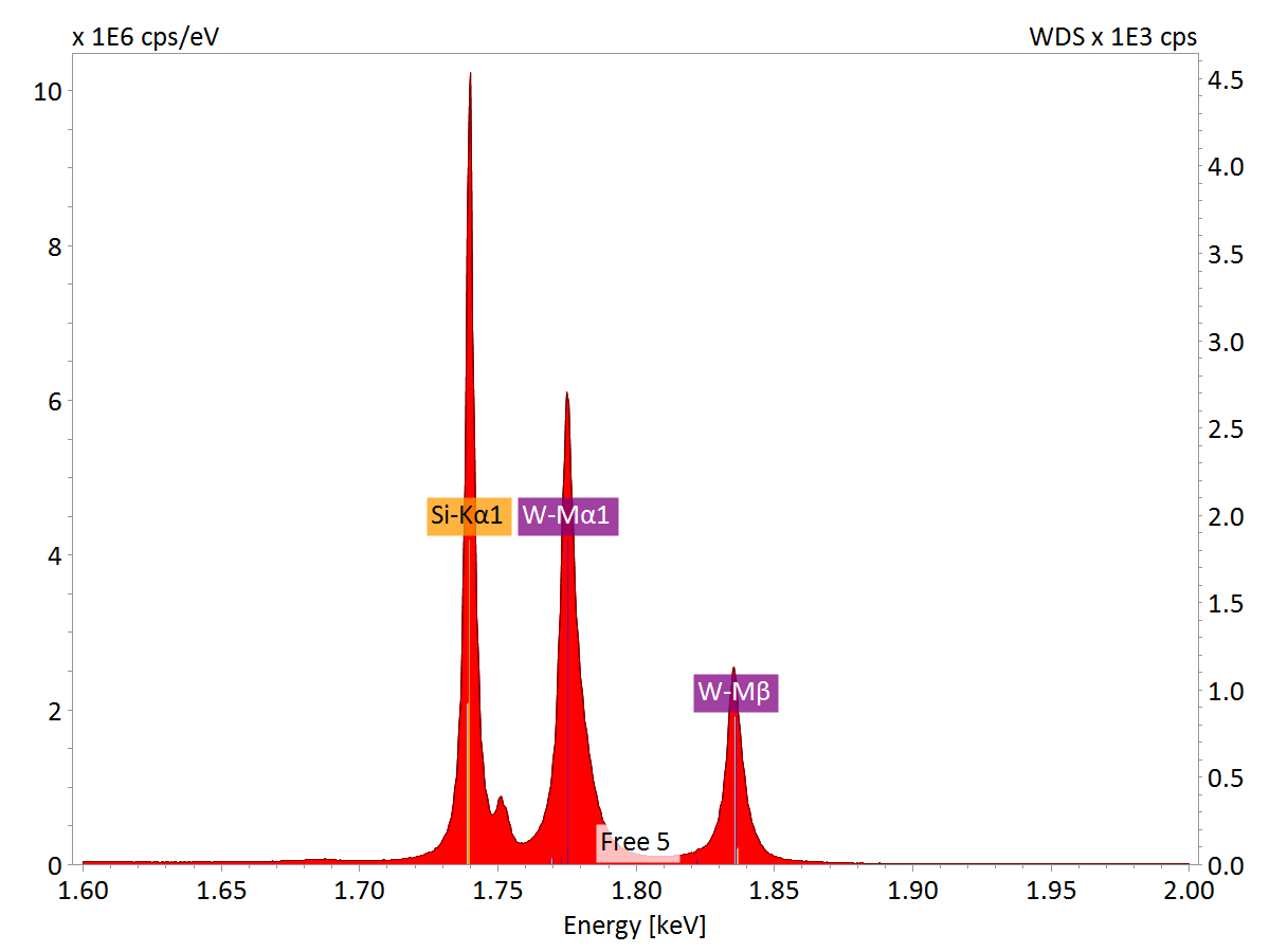
To in quality control of micro and nano level in the high spatial resolution, materials must be accelerated to low voltage is analyzed, and the premise that the phase identification difficult.In this case, the line is W M spectrum peak can be inspired, and the spectrum summit and Si substrate material line is K + serious overlap.
The resulting main elements (Si) of EDS peak will widen, and conceal the existence of the second phase (W).Corresponding, if useQUANTAX WDSAnalysis, due to its remarkable energy resolution, W and the recognition of the Si each peak can be perfect.