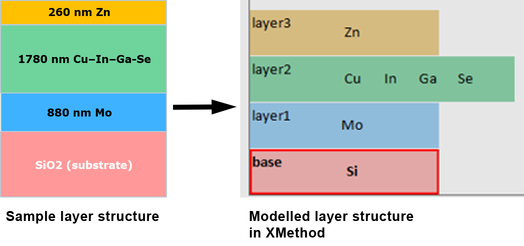
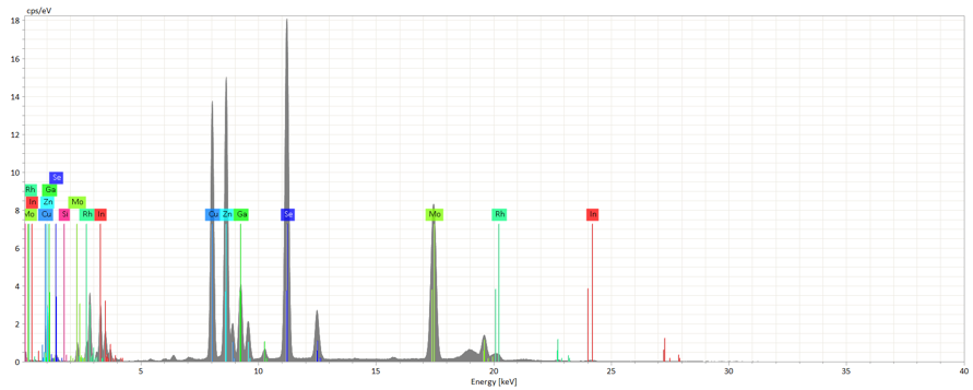
SEM micro zone XRF analysis of the film

When the x-rays can pass through matter, they X-ray fluorescence (XRF) can be used to determine the film thickness.inTo use the micro area XRF SEM,On the micron scale analysis of thin film layer (thickness and composition) possible.Is very dependent on film thickness analysis based on quantitative parameters (FP) the basis of material atoms.Through the use of standard sample, the various types of layer system can through the research of standard sample such as wafer metallization, metal coating pretreatment and solar cells.When standard samples are available, SEM micro area of XRF analysis can greatly improve the accuracy.Sometimes even if there is no standard sample, rely on the element FP data information, we can also analyze the film layer, such as test of the new film system development environment, such as solar cells (figure 1).

Figure 1: solar cells, thin film sample analysis.in大多数情况下,吸光层是CIGS层,CIGS结构是Cu-in-Ga-Se或Cu-in-Ga-S化合物。CIGS-太阳能电池通常由涂有 Mo 层的玻璃基板上的沉积制成。与SEM的传统薄膜厚度分析相比,XTrace在不需要在横截面模式下测量层,它可以直接在平面上测量SEM样品厚度。这是一种快速、无损的技术,无需样品制备。
Figure 2: the micro area of solar cell XRF spectra showed that all the relevant elements from different depth of spectral lines, or even below the surface of the sample ~ 2 microns Mo can be detected.Line is important to note that high-energy heavy elements (such as Mo - K and the In - K) can be XRF excitation source easily.And X-ray source excitation depth is big, inside the material elements can be more in-depth observation, so that they can to relatively thick film even multi-layer system from 1 nm to characterization of 40 microns.In addition, it also can make decisions about the composition of the structure of CIGS.This case USES the top base parameter method is analyzed.Using standard samples to improve the accuracy.