ContourX - 200 optical profiler provides advanced characterization ability, can be selected system accessories, and the perfect combination of easy to use, is of similar products in the fastest, the most accurate, high repeatability of non-contact 3 d surface measurement system.Cover an area of an area small, the measurement system using a larger field of view, 5 mp digital camera and a new electric XY worktable, has excellent ability of 2 d / 3 d high resolution measurement.ContourX - 200.拥有出色的 Z 轴分辨率和精确度,具备布鲁克专有白光干涉(WLI)技术广受业界认可的所有优势,而且不存在传统共聚焦显微镜和同类普通光学轮廓仪的局限性。
ContourX - 200 optical profiler relying on more than 40 years of index of independent innovation achievements, can meet the required quantitative measure low noise, high speed, accuracy and precision.Through the use of a variety of objective and pattern recognition, can the nano vertical resolution in multiple view tracking characteristics, for the quality control and process monitoring and application of multiple industries provide is not affected by the size of the result.ContourX - 200 on the surface reflectivity of 0.05% to 100% of all cases could play a stable performance.New hardware features include innovative design workbench to obtain greater joining together;A 5 mp camera, using 1200 x1000 measuring array, low noise, larger view and higher lateral resolution.
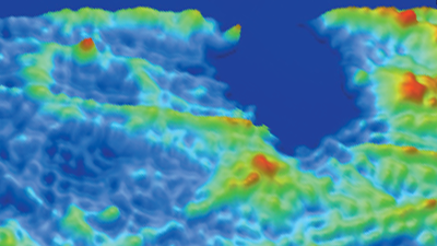
The white light interference all objective to provide a constant vertical resolution.
The most widely used analytical capability
X - 200 electric level.
ContourX - 200 USES the powerful VisionXpress and Vision64 user interface, providing thousands of custom analysis to improve the efficiency of the laboratory and factory.Brooke new general scanning interference (USI) measurement mode can provide fully automatic, since the perception of surface texture, optimization of signal processing, the surface morphology of the analyzed performs the most accurate, the most practical calculation.The system USES the new camera, enlarged the field of view, combined with new electric XY worktable with flexibility, improve the flexibility of dealing with a variety of samples and parts and efficiency.The perfect combination of hardware and software, to achieve excellent optical performance, comprehensive beyond the similar measurement technology.
application
application
Surface - Independent Metrology with Application - Specific Solutions
Precision Engineering
Keep the surface texture and geometric dimensions of precision - engineered parts within tight specification limits. Our gage - capable measurement systems dojo.provide efficient feedback and reporting as you monitor, track, and evaluate the processes and assess GD&T conformance.
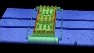
MEMS and Sensors
Perform high - throughput, highly repeatable etch the depth, film thickness, step - height, and surface roughness measurements, as well as the advanced critical dimension metrology of MEMS and optical MEMS. Optical profiling can characterize devices throughout the manufacturing process from wafer to final test, and even through the transparent packaging.
Orthopedics/Ophthalmics
Obtain precise and repeatable measurements of impla雷竞技网页版nt materials and components through the complete product life cycle. Our index optical profilers support R&D, QA, QC and analyses, the for applications held characterization of surface parameters of lens and injection molds to surface finish verification and wear of medical devices.
Tribology
The Measure, analyze, and control the impact of friction, wear, lubrication, and corrosion on the material/component performance and lifespans. Determine policy wear parameters and perform fast pass/fail inspections on the widest range of shiny, smooth, or rough surfaces.
Semiconductors
Improve yield and reduce costs for both front and back - end manufacturing the processes with automated, non - contact, wafer - scale metrology systems. Perform post - CMP die flatness inspection;Bump height, coplanarity, and defect identification and analysis;And measure the critical dimensions of component structures.
called
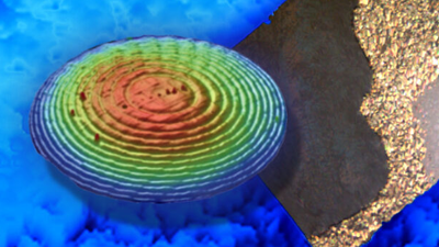
Better understand the root causes of the defects and optimize polishing and finishing the processes with accurate and repeatable sub - nm roughness measurements. Our non - contact metrology systems enable the compliance with his stringent specifications and ISO norms for samples held small aspheric and free - form called, to optical components with complex geometries', to diffraction gratings and microlenses.